
Semiconductors, such as silicon, they themselves donnot conduct electricity, so we have to add impurities to the material. (We call this process doping) There are two types of doping, n-type and p-type.
We add Phosphorus which is a Group XV element meaning it has 5 electrons but only 4 of them are needed to form a covalent bound with sillicon so we have one extra electron floating around. IMPORTANT: Notice that here the doped material does not carry any overall charge! It is Phosphorus atom being added not ion, so the overall charge is zero.
A word on naming: Since in this case, the substance has negative charge floating around, we call it n-type.
We add Boron to Silicon in this case. Since Boron has three electrons on the outmost shell, it would make the BSi4 structure lack one electron to form all 4 covalent bounds. In this case we say that the structure has a hole in it, which is basically a space for a electron. Notice that, again, we don't have a overall charge on our material.
These are two currents formed by a pn-junction. We will first need to explore the electric field formed by this. So before we put the pn junction into one piece, they are neutral individually by themselves. At the time we put them together, a diffusion current occurs. Then the positively doped side has electrons from the other side so the p-type side is now overall negative in charge (with extra electrons), and the n-type matreial is now overall positive in charge (short in electron). ... This causes an electric field. In an electric field, a electron is given a force to move from the negatively charged side to the positively charged side, and the current caused by this movement of electrons is called a drift current.
A Diffusion is the current of electron moving from n-type doped material to p-type doped material. (一开始电子填补空洞而产生的电流) In conventional current this goes from p to n. A Drift is the current formed by electron being 'sucked' back under the force of the electric field. (后来电子因为电场的作用而从负极到正极所产上的电流) In terms of conventional current, it goes n -> p.
A word on naming: A way to think of the naming is: diffusion means to spread, to even out so it is the process of evening out the electrons/holes in the materials. And a drift could be thinked in the way that electrons have moved from p->n now they have to move back n->p, so the electron needs to 'drift' to make a u-turn.
A Equilibrium will be achieved eventually, this is intuitive. We call the layer of 'neutral' layer in a pn-junction a depletion layer.
+[P-type|n-type]-
In this case:
Hence the application of voltage decreased the depletion layer and made the pn-junction conductive.
-[P-type|n-type]+
In this case the p-type end, which is originaly more negative, gets negative, which means gaining more electron so it further increases the width of the depletion layer. (Similar for the n-type end) So all in all, the depletion layer increases and hence the pn-junction becomes insulating.
Metal Oxide Semiconductor Field Effect Transistor; There are two types of nMOS and pMOS; Notice that in both nMOS and pMOS, if we don't apply any voltage to them, the transistor acts as a two way insulator since at least one way the depletion layer will increase.
The nMOS is formed by a npn combination of deoped semi-conductors. There is a metal connection (The M in MOSFET) called gate at the top of the p-type substrat. When a 5V voltage is applied to the gate, electrons will gather at the top of the p-type substrat and then the two n-type substrats are connected through this n-type channel.
The pMOS transistor is formed by a pnp combination of doped semi-conductors. Generally the same as the above case. Note: logic zero is differect from not applying voltage!!! Only zero voltage applied will cause the positive charges to gather at the top and allow a p-type channel hence allowing conducting electrocity.
This quora answer explained these two concepts well and I hereby ackowledge that I quoted this answer in my explaination.
A standard truth table is a truth table such that the first column of input has first half equal to zero and second half equal to to one; the sencond column is divided into two parts the upper half and the lower one and in each half: the top half is zero and lower half is filled with one; and on and on and so on... The verbal description may be hard to understand, we shall see this through a example. Say we have three inputs A, B and C with one output Y.
| A | B | C | Y |
|---|---|---|---|
| 0 | 0 | 0 | |
| 0 | 0 | 1 | |
| 0 | 1 | 0 | |
| 0 | 1 | 1 | |
| 1 | 0 | 0 | |
| 1 | 0 | 1 | |
| 1 | 1 | 0 | |
| 1 | 1 | 1 |
Minterms are rows in a standard truth table that has a one as output. They are labled with index, starting from the first row as index zero. A minterm is a product (AND) of all variables in the function, in direct or complemented form. (Intuition hehind naming:) A minterm has the property that it is equal to 1 on exactly one row of the truth table.
Formal: an AND expression with every input present in true or complemented form. So for example given inputs A, B, C and D, valid minterms could look like or et cetra, et cetra.
Maxterms are rows in a standard truth table that has zero as output. A maxterm is a sum (OR) of all the variables in the function, in direct or complemented form. A maxterm has the property that it is equal to 0 on exactly one row of the truth table.
Formal: an OR expression with every input present in true or a complemented form.
min 0\bar{1}
In case of min term, if it is with bar, then it is one. W/o bar means zero. Min has first syllable m so 0和1中的min‘没’有bar
max \bar{0}1
In case of max term, if it is with bar, then it is zero. W/o bar means one. Max has first syllable M so 0和1中的Max‘没’有bar
Sum of Minterm is a way of expressing which inputs cause the output to go high under the assumption that the index is the index of the row in a standard truth table. This method gives us a more compact way to display the entire truth table. Sum of Minterms are useful in calses with very few input combinations that produce high output. While Product of Maxterms is useful when expressing truth tables that have very few low output cases.
An interesting property is that , Minterm x is the complement of Maxterm x. For example: . We can also convert min/max term back and forth. For example a 2-input XOR gate has SOM form and this is equivalent to the POM form which indeed the XOR gate.
and
and
and
and
and
K-maps are 2 dimensional grid of minterms, where adjacent minterm locations in the grid differ by a single literal and the values in each grid is the output for that combined minterm.
Once a K-map is created, draw boxes over groups of high output values subject to the following constraints:
There are two types of adders, the hald adder and the full adder respectively. We will take a look at them respectively below.
Half adders are cheaper to implement. They have two bits for the to input bits that are to be added and and two bits for ouput, one for carry out and one for the added bit output. (adds to bits to produce a two bit sum). One might find that the logic circuit is overwhelming in terms of memorizing, but it falls apart if we look at the logic expression: and where we remember that represents the carry bit and is the main output bit.
Full adders are slightly more complicated then half adders since they have an additional bit of input that takes care of the carry input. Same as above, we can use the logic expression to remember the logic circuit level design, which is as follows and where we remember that represents the output and carry respectively.
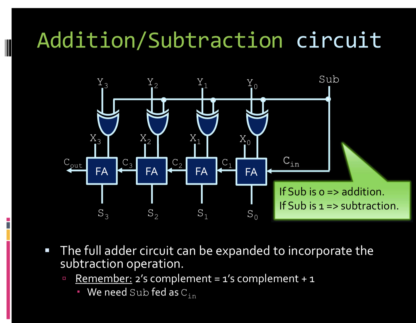
Subtractors are an extension of adders. Basically we perform addition on a negative number. Befpre we do subtraction, we need to understand how negative numbers work in binary settings.
(000001 -> 111110 -> 111111)Since we perform subtraction in the form of adding a negative (2's complement) number, we can create a subtraction curcuit based on this. To do so, we will rely on the same set up that we had in the case of ripple adder. We will add a negation gate to each of the bits from the number to be subtracted (1's complement) and input a 1 at the carry bit for the first full adder (2's complement).
This is rather hard to explain in plain english, so I borrowed Prof. Steve Engels' slide
def: A circuit that takes in two input vectors, and determines if the first is greater than, less than or equal to the second.
The most basic arithmetic comparator would probably be the one for two bits. The circuit for the two inputs A and B would be
Anyhow, the general comparator's could be cumbersome to write down, since you will still need to define an equation for each case.
As number of digits that we need to compare gets larger and larger, the comparator circuit gets more complex. At a certian level, it can be easier sometimes just process the result of a subtraction operation instead. (This is easier to implement, just it is not any faster).
So far, we have looked at combinational circuits: circuits where the output values are entirely dependent and predictable from current inputs. Another type of circuits is sequential circuits which are circuits that also depend on both the current inputs and the precvious state of the circuit.
Essentially, sequencial circuits are a result of having feedback in the circuit. We want to feed the output of a circuit back into itself as a new input and this accomplished thanks to Gate Delay. Gate Delay: (aka Propagation Delay) Even in combinational circuits, outputs don't change instantaneously. The delay is defined as 'The length of time it takes for an input change to result in the corresponding output change'
We will begin by looking at some examples that fails to be useful.
In this case we feed the output of the and gate back to itself as a new input. At any stage, regardless of what we feed into the circuit (into the one input left) the output will always be logic low. So this circuit is stucked at zero and cannot change.
In this case, if we ever give the input a logic high, then the output will be locked as logic high and regardless of input, the output won't change. So, again a dead state, not really useful.
Let's call the input , and the fed back wire ; Assuming that we set to be 0, then the output will be 1 (we want this). If we set , the the would alternate its value between zero and one (we don't want this/ unsteady state, can't store for a long time).
Let's call the input and the fed back wire ; Assuming that we set to be 1, then the output will be zero (we want this). If we flip , then the output will alternate between 0 and 1 (don't want this).
If multiple gates with feed backs are combinaed we can get more steady behavior! And these circuits are called latches.
Word on naming: The S and R in the name corresponds to Set and Reset. As a convention, in circuits we call setting and reseting.
It is rather hard to describe the circuit in words so shall describe it's behavior here as a memory cue.
In this case, the inputs are and . Notice that the bar identifies these two ports as active low, which means zero is active. In this acse, if we have the input the is zero, which means it is 'triggered' and the output is 'Set'. The other way around holds for the case where where the 0 triggers 'reset'(). For a latch to lock the value, we need to set . There is a handy way of remembering this. Since here we are having active low on our inputs, and (forbidden state) makes the output set and reset at the same time, which makes absolutely no sense. would be not doing anything, and hence holding the state.
In this case, the inputs are and . Notice that in this case there is no bar, so they are active high, which is the normal case. If we have input then the sets, and resets. Simmilar to the case above, there is one forbidden state -- we can't set and reset at the same time ( forbidden) and neither resetting nor setting () holds the state.
In the two sections directly above, we have defined the forbidden states for each sort of latche. Notice that they are forbidden because they can cause unpreditable behavior since in actual circuits lags are real things and we can't tell in a flip from or which one of the two bits will actually flip first!
Now we have circuit units that can store high or low values. How can we read from them? (Interesting question: if we receive a logic high, how do we tell if it was meant to be a single high value or it's two high values in a row?) This is where clock signals come into play. Definition: Clocks are a regular pulse signal, where the high value indicates when to update the output of the latch.
The limit to how fast the latch circuit can be sampled is determined by
Adding another layer of NAND gates to the latches yields us the clocked latch. The new layer has a 'controller' called or sometimes a gate. Here, when the gate receives logic high, the latch's value could be changed/updated and when the gate takes zero, the entire component is essentially locked (no change allowed).
This latch is formed by adding another layer to the clocked SR latch: we use a single source for purpose of setting and resetting. The single control is connected to and (using a negator) is connected to R. This way, the latch won't ever run into the forbidden states. This design is overall good but it still have problems, for example, timing issues.
Transparent means that any change to its inputs are visible to the output when control signal (Clock) is 1. The take away: The output of a latch should not be applied directly or through combinational logic to the input of the same or another latch when they all have the same control (clock) signal.
A flip-flop is a latched circuit whose output is triggered with the rising edge or falling edge of a clock pulse.
The above SR flip flop still have issues of unstable behavior. We can solve this by using a D flip-flop.
This acts like a dff, except it flips rather than sets meaning that toggles to the opposite value whenever the input to T is high.
The all in one flip flop with two inputs J and K.
In the FSM settings, a machine is safe if it doesn't cause a glitch to happen. For example in a FSM with states 00, 01, 11 if I can transit from 11 to 00 directly, then I don't know which bit of state F will flip first. This is problematic, we want safe machine assignments!